5. Electronics production
Group Assignment
This week, we had to document these parts:
Characterize the design rules for your in-house PCB production process: document feeds, speeds, plunge rate, depth of cut (traces and outline) and tooling.
The workflow for sending a PCB to a board house
Here is the link to our group assignment page.
Individual Assignment
This week I worked on making and testing my desgin circuit board with seeed studio XIAO-RP2040.
1. Milling my design circuit board
a. Preparing
I used ProtoMat S103 milling machine from LPKF Laser & Electronics.
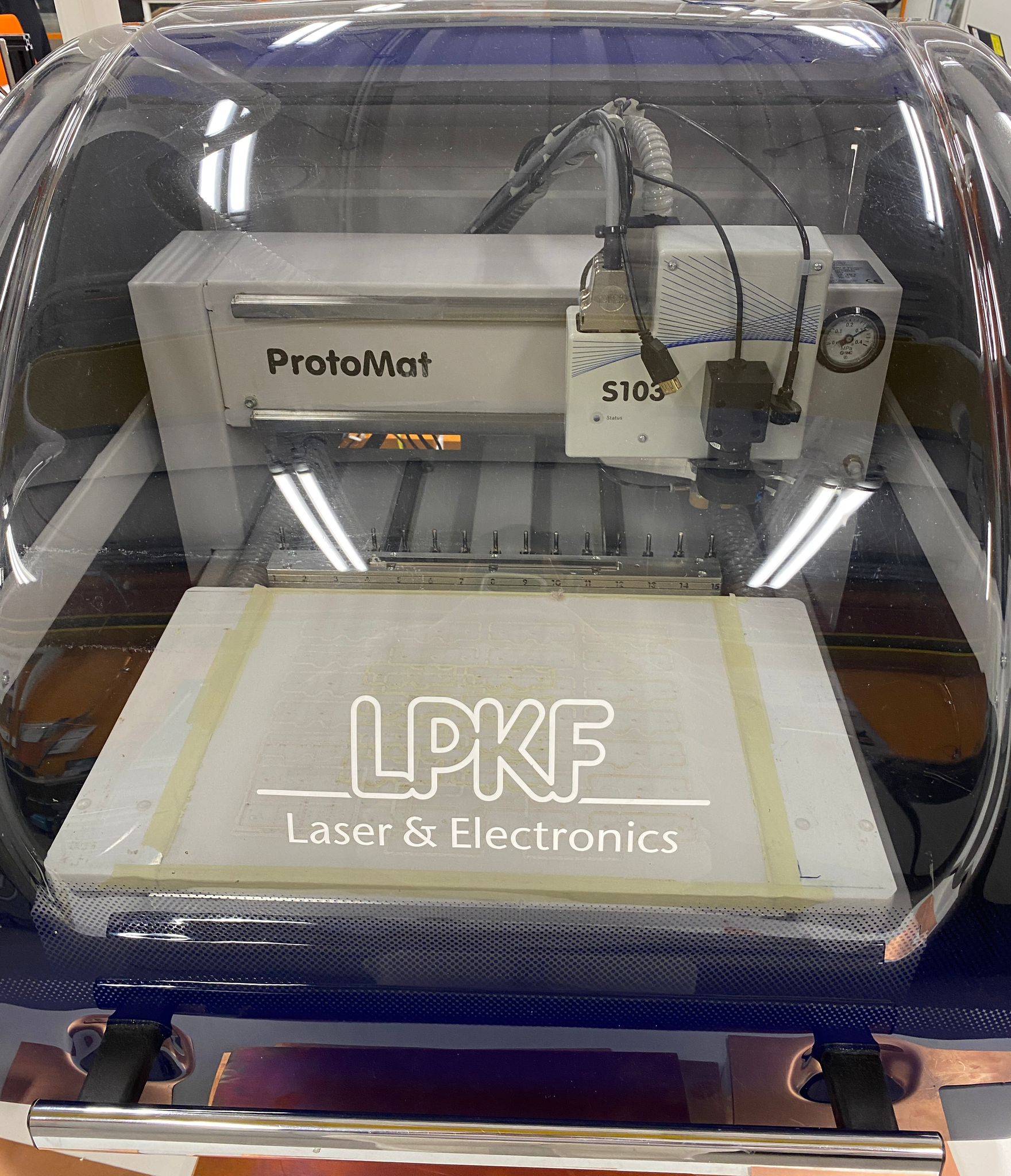
First, I experted my pcb file into gerbers (.gbr) which will have 1 F_Cu file and 1 Egde_Cuts file, in order to milling my board and cut my board from a big FR4 plate. After I copy those files from my laptop to the computer connected with the machine, I started with setup the machine.
b. Setup and processing
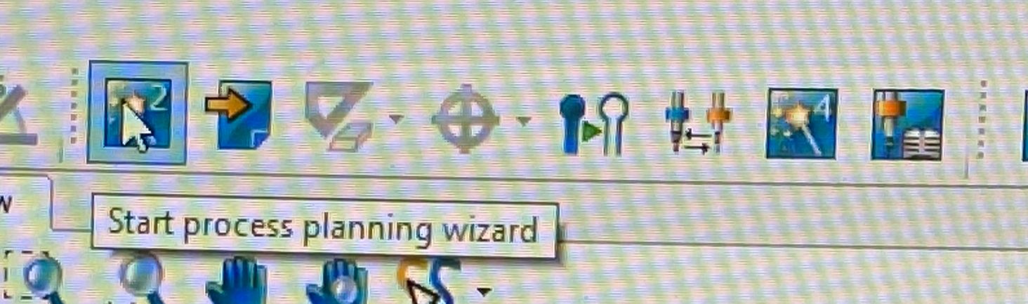
1.Start process planning wizard
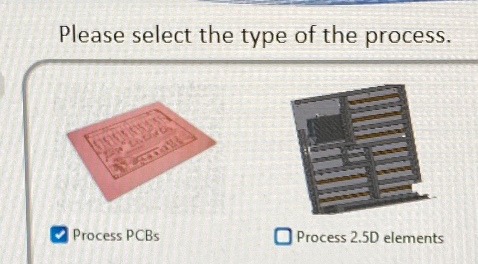
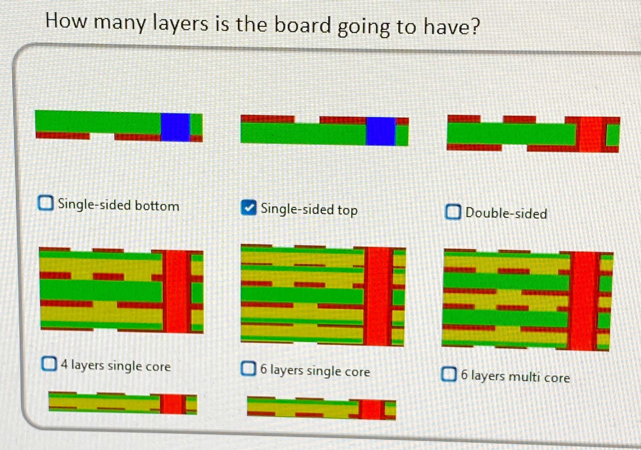
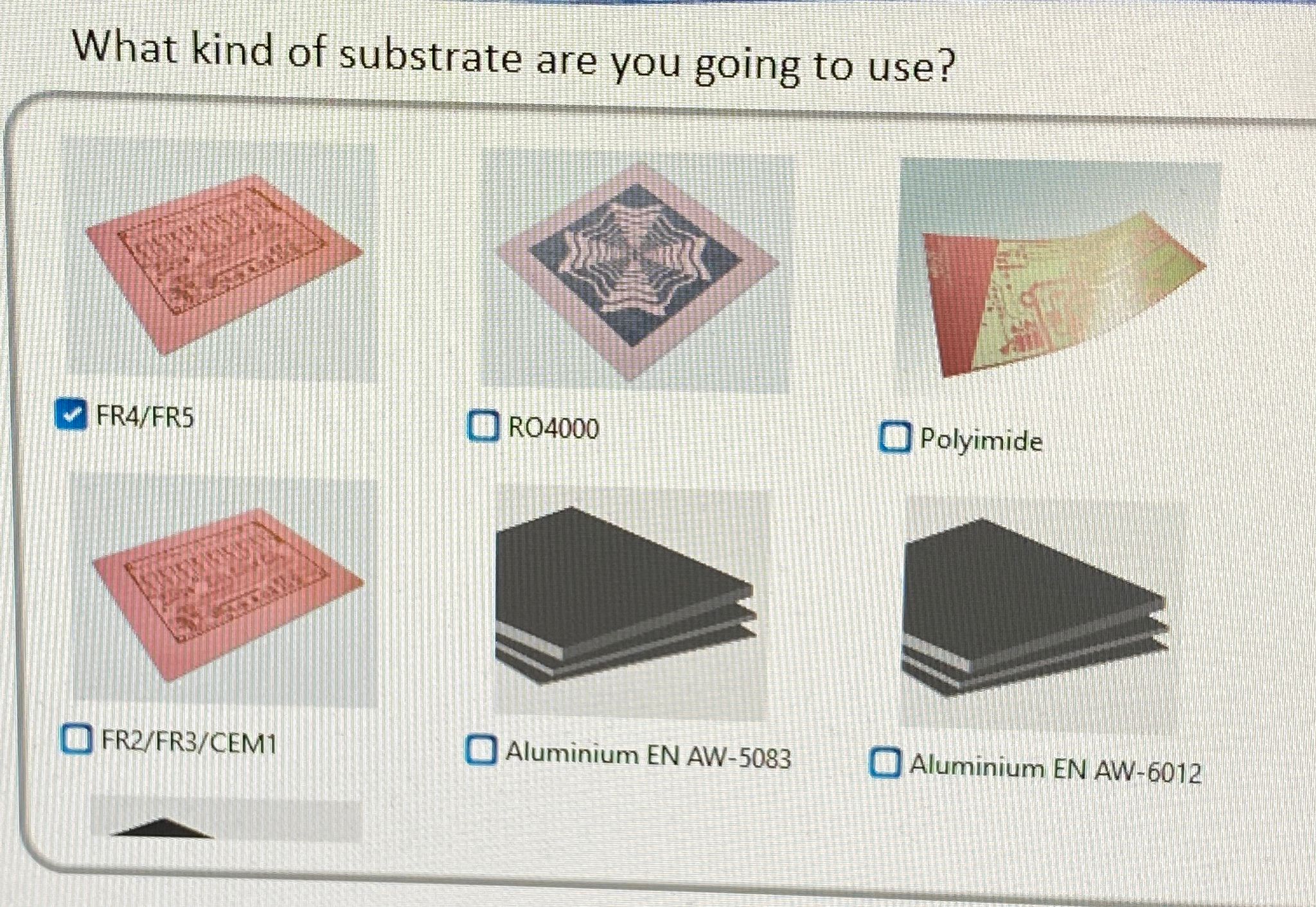
I choosed: Process PCBs -> Single-sided top -> FR4/FR5
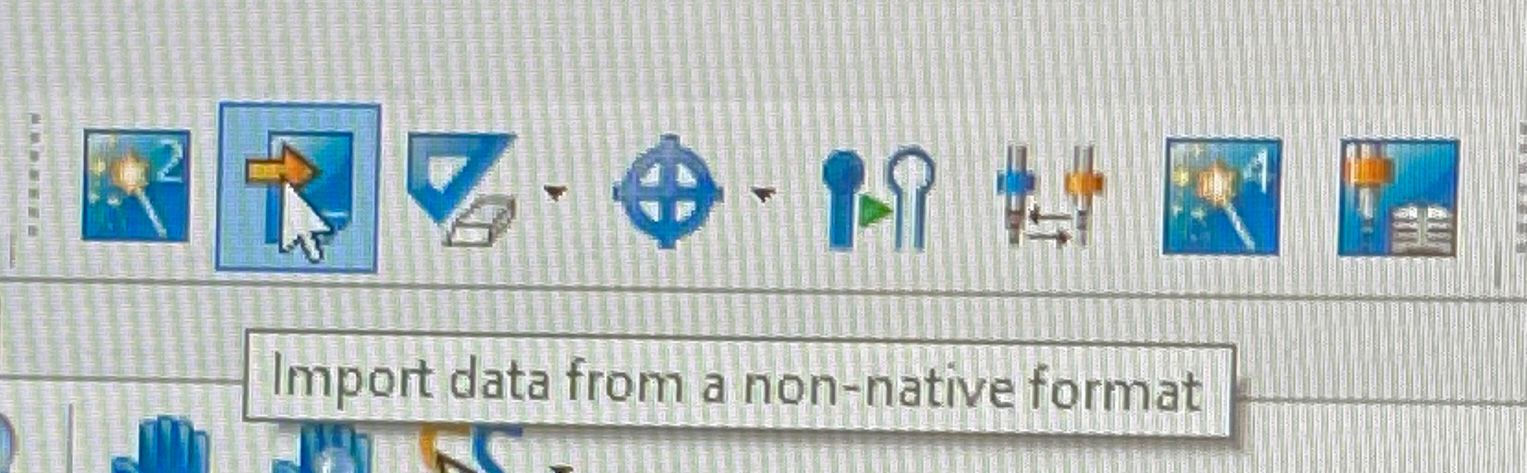
2.Import data from a non-native format
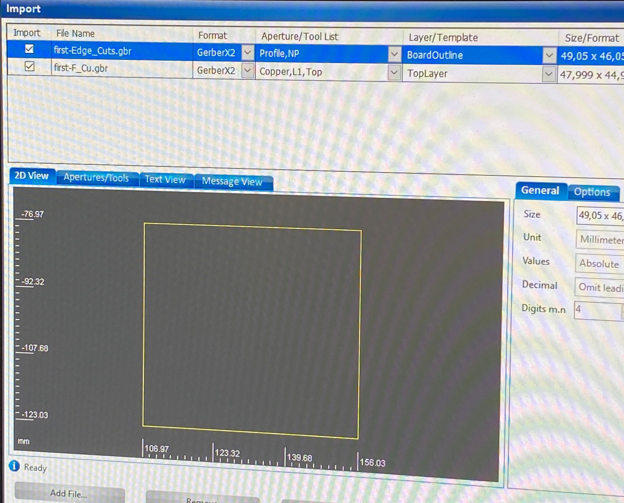
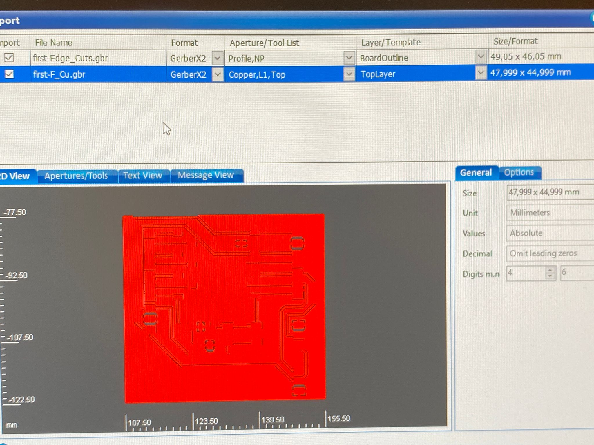
At this step at import two gerber files from computer to the applicant. Then, two files will be shown with 2D view
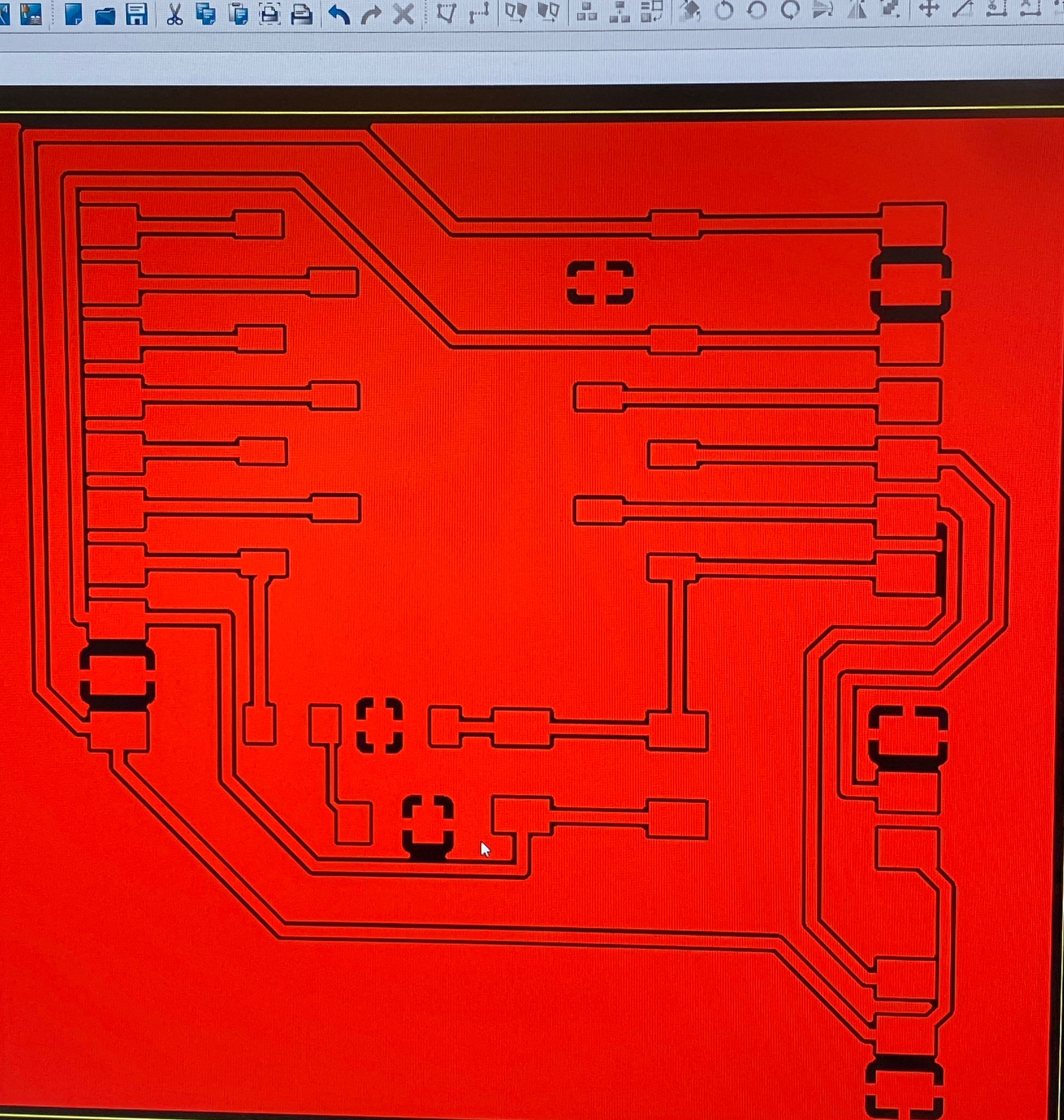
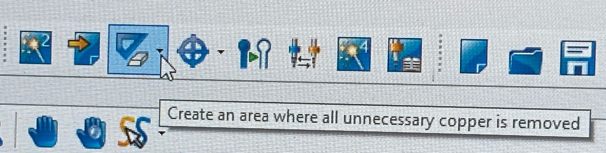
3.Create an area where all unnecessary copper is removed
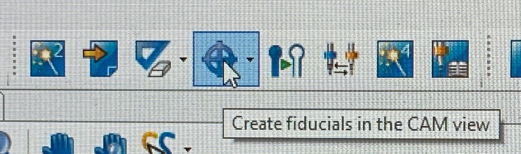
4.Create fiducials in the CAM view
These two steps were skipped in my design because i do not need these but I still consider later for my next milling.
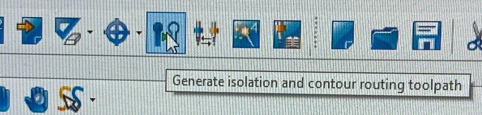
5.Generate isolation and contour routing toolpath
At this step, I will isolate paths and pins from the GND, and choose how to cut the Edge_Cuts path.
There are two recommended choices for isolation: Basic and Pads Double
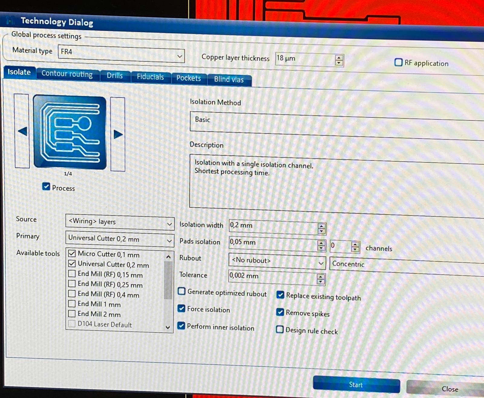
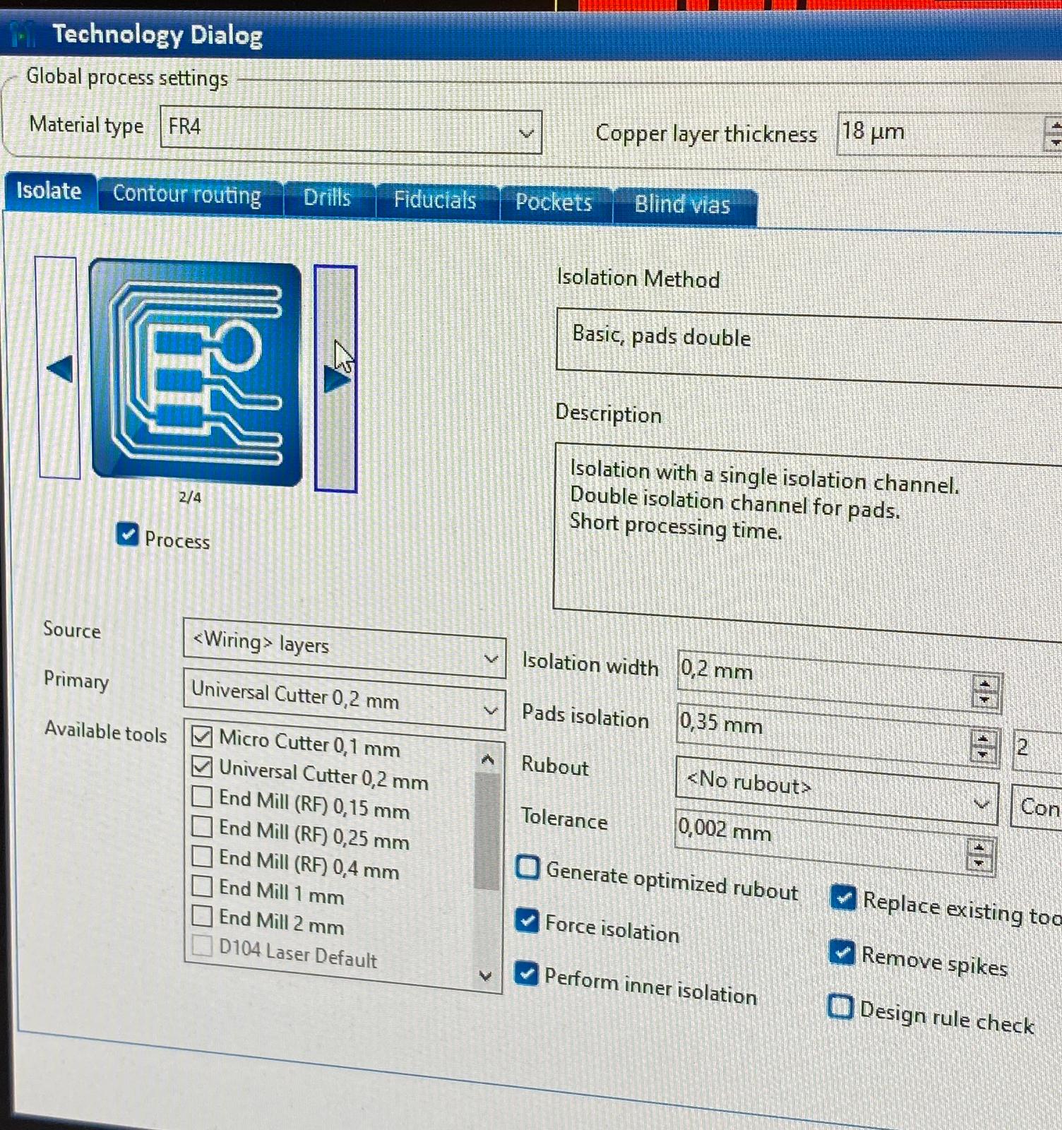
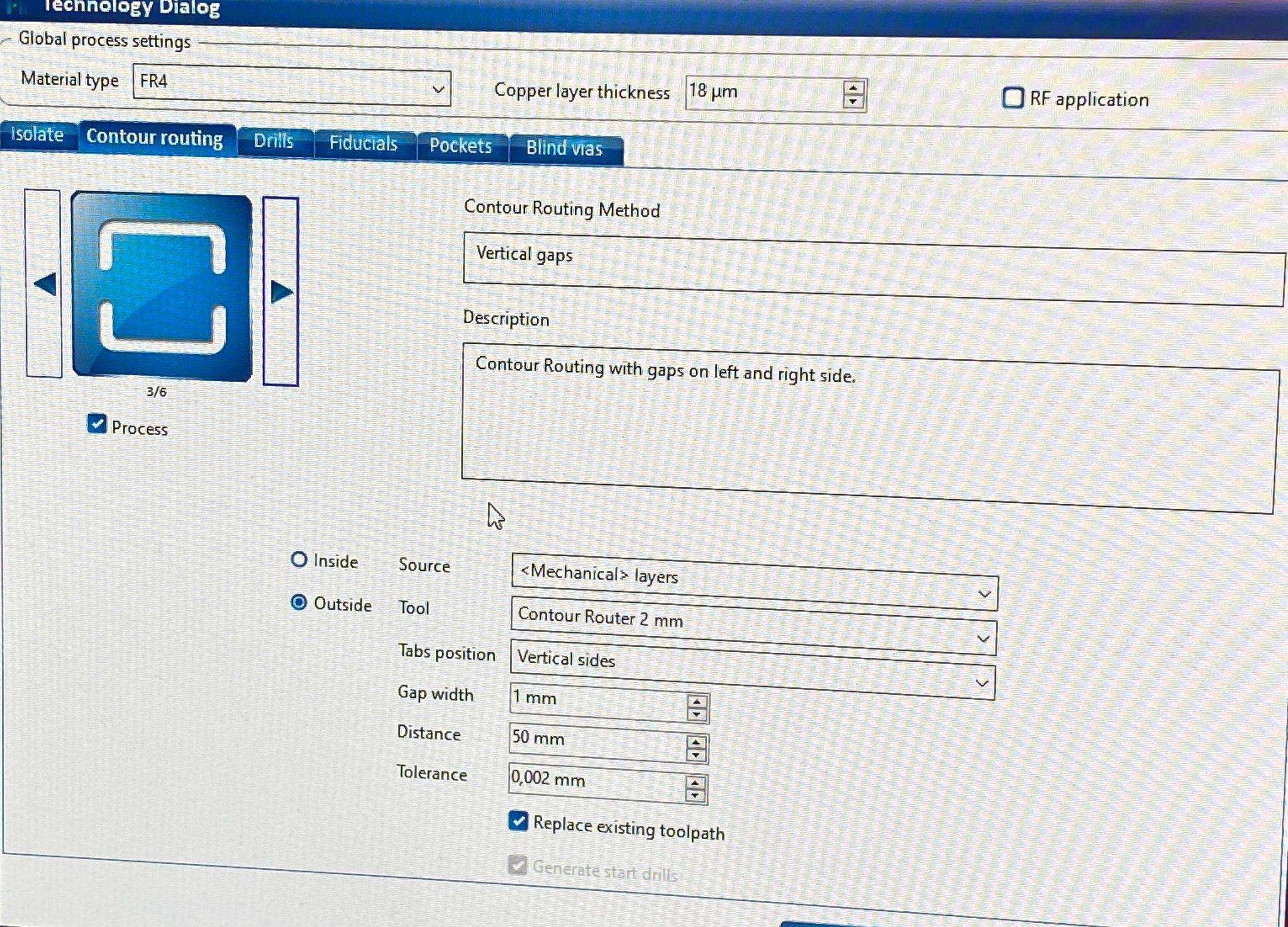
Next, Contour routing. There are six different ways to choose, but i chose Vertical Gaps.
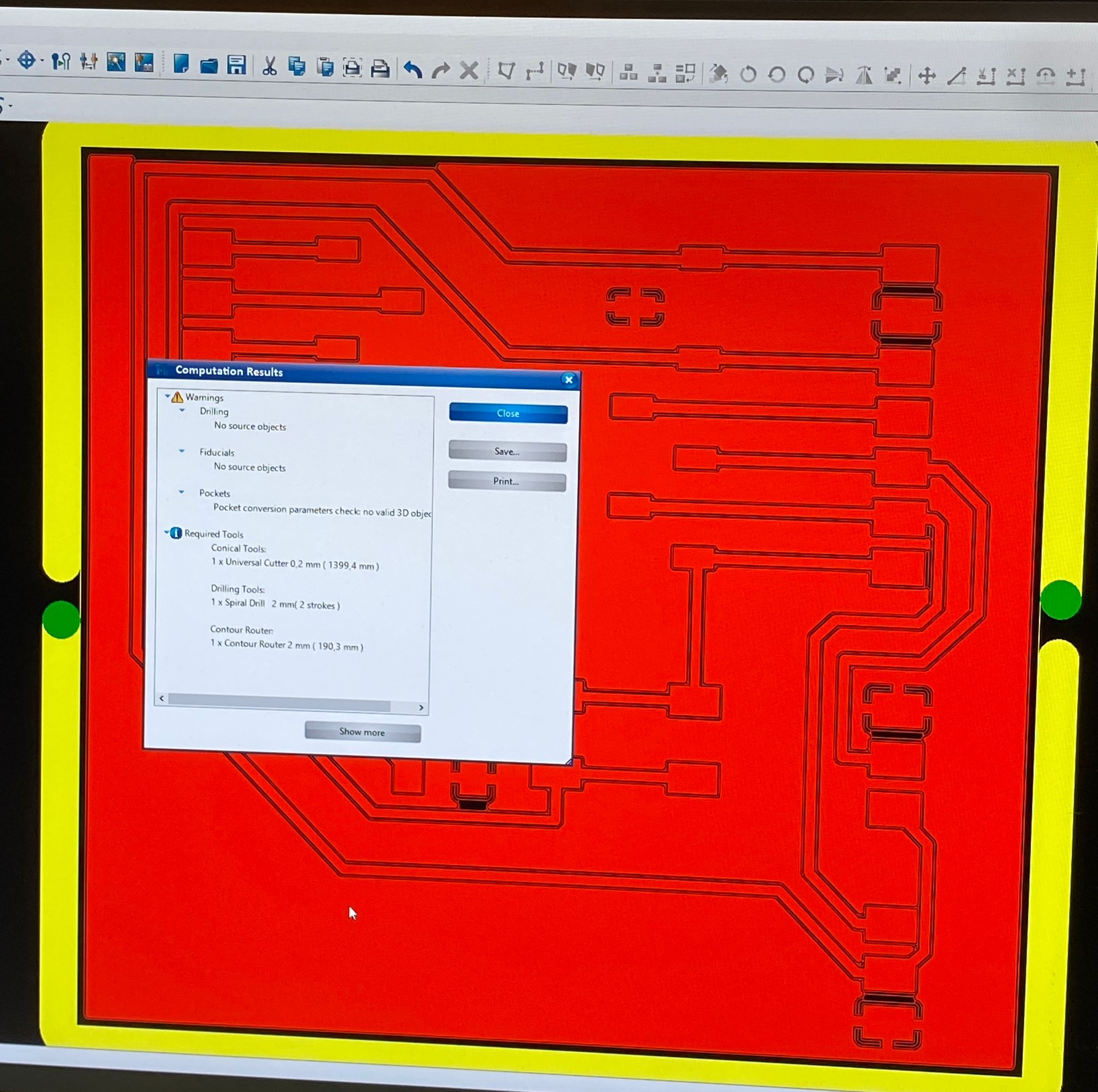
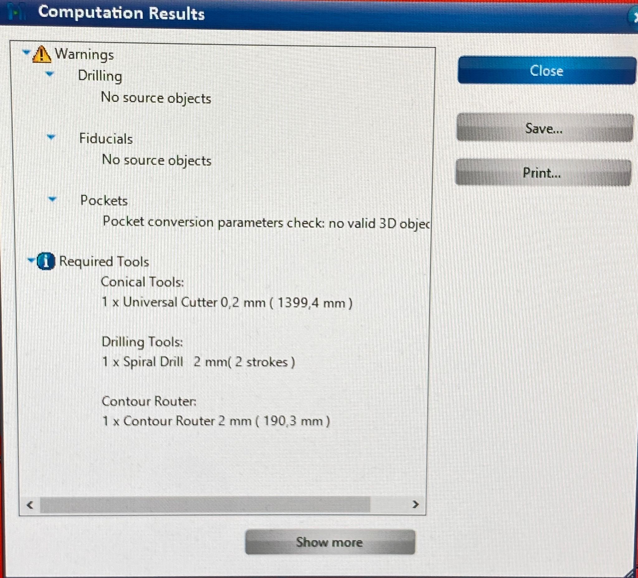
After finish this fifth step, the software showed how my circuit board was milled, cut and required tools for the process.
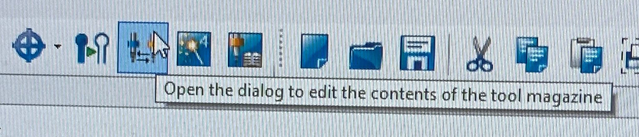
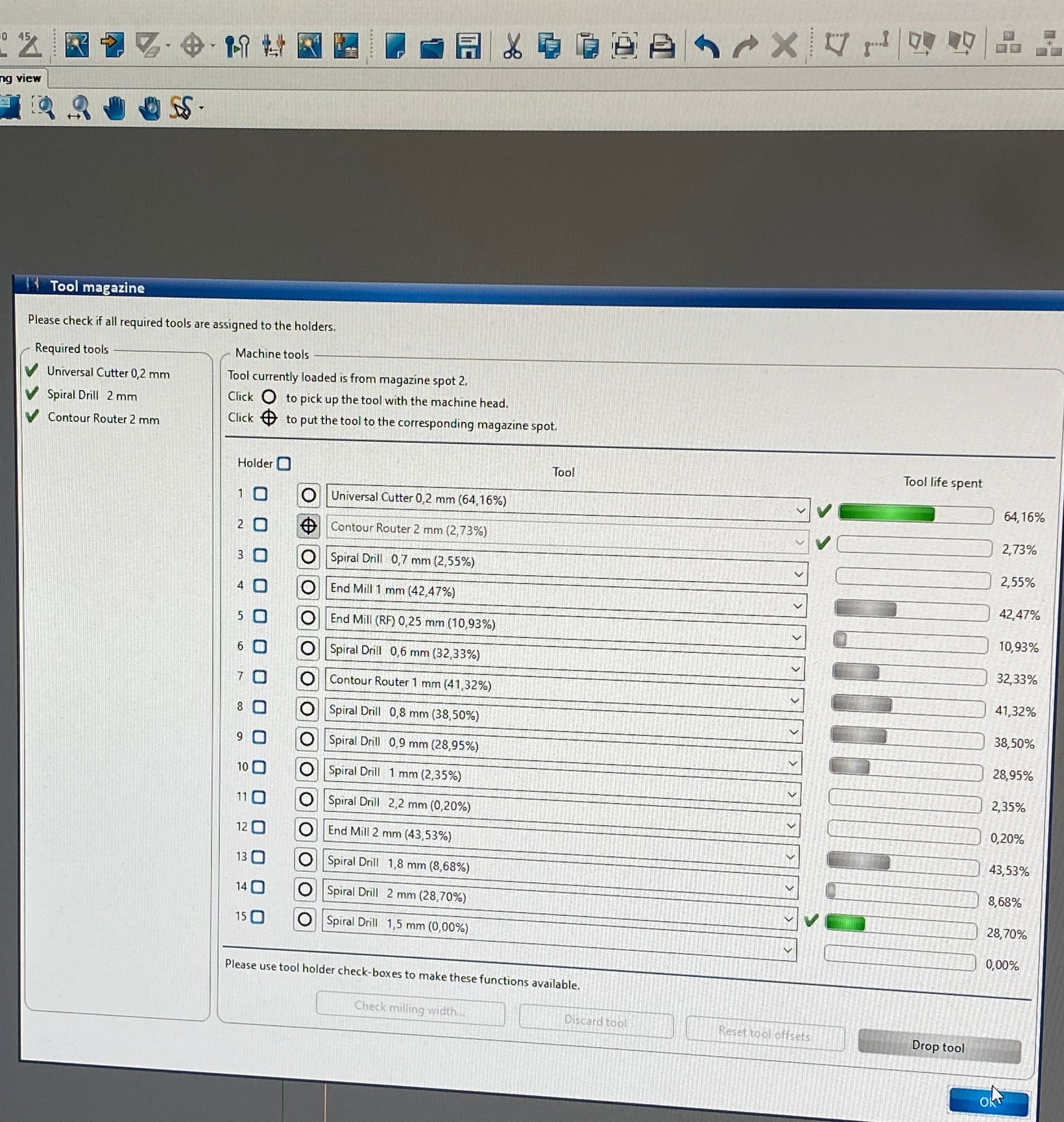
6.Open the dialog to edit the contents of the tool magazine
In the step, the software show about the required tools for my design is still able to mill and cut or need a new replacement.
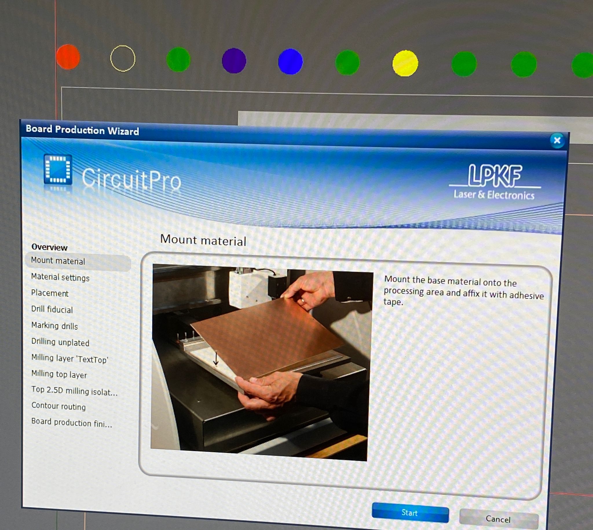
7.Start the Board Production Wizard
There are many stages for this step:
Mount material
 Material settings and Location
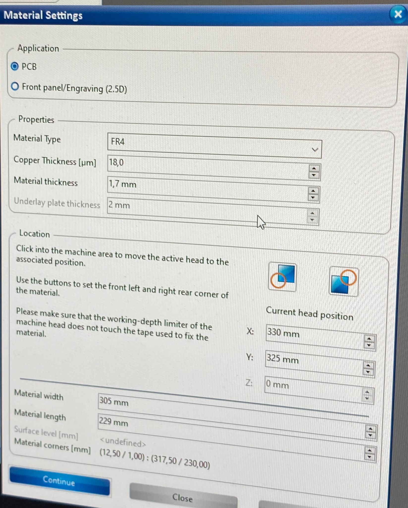
Processing with XYZ-positioning
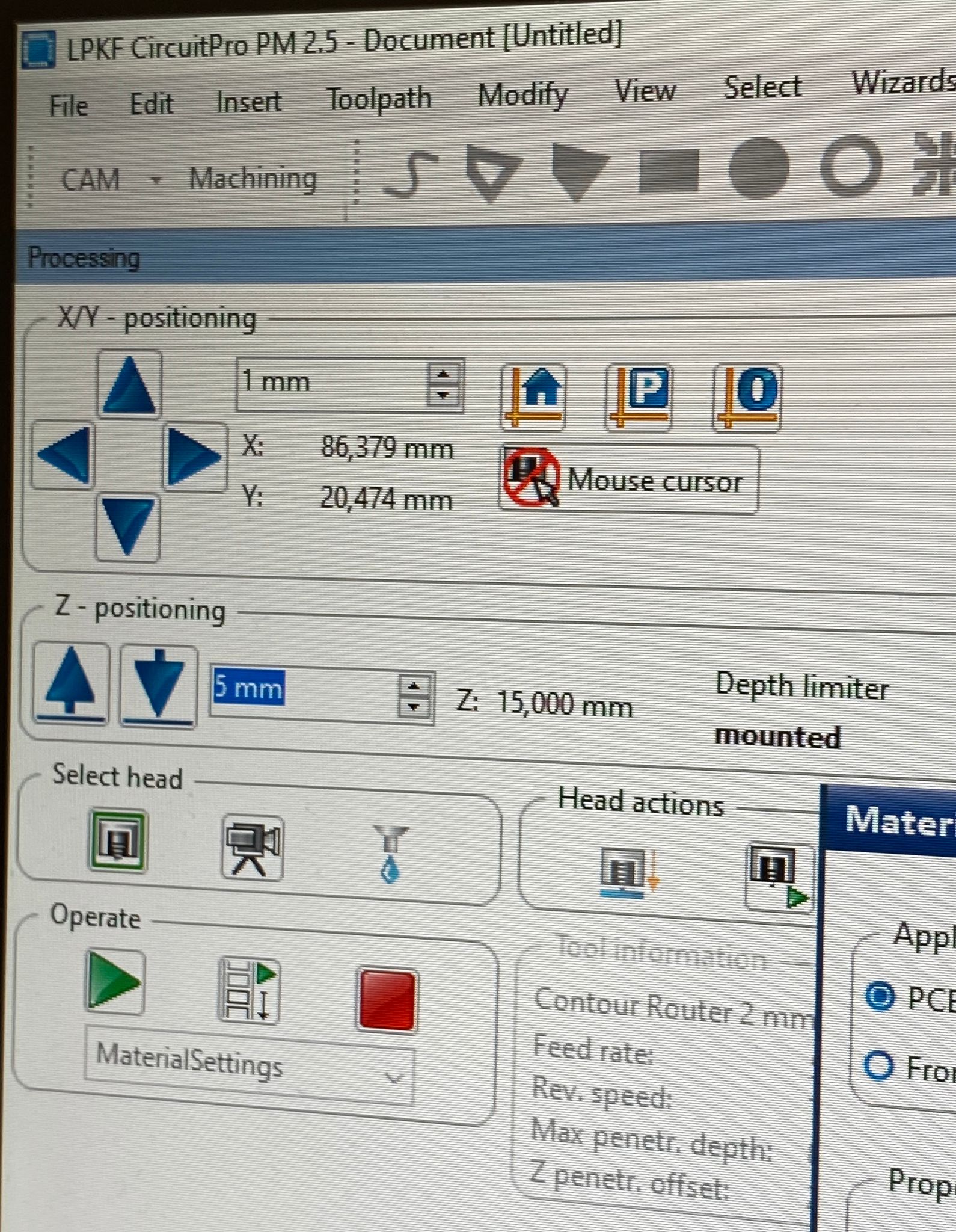 I move it to find a good location for my design
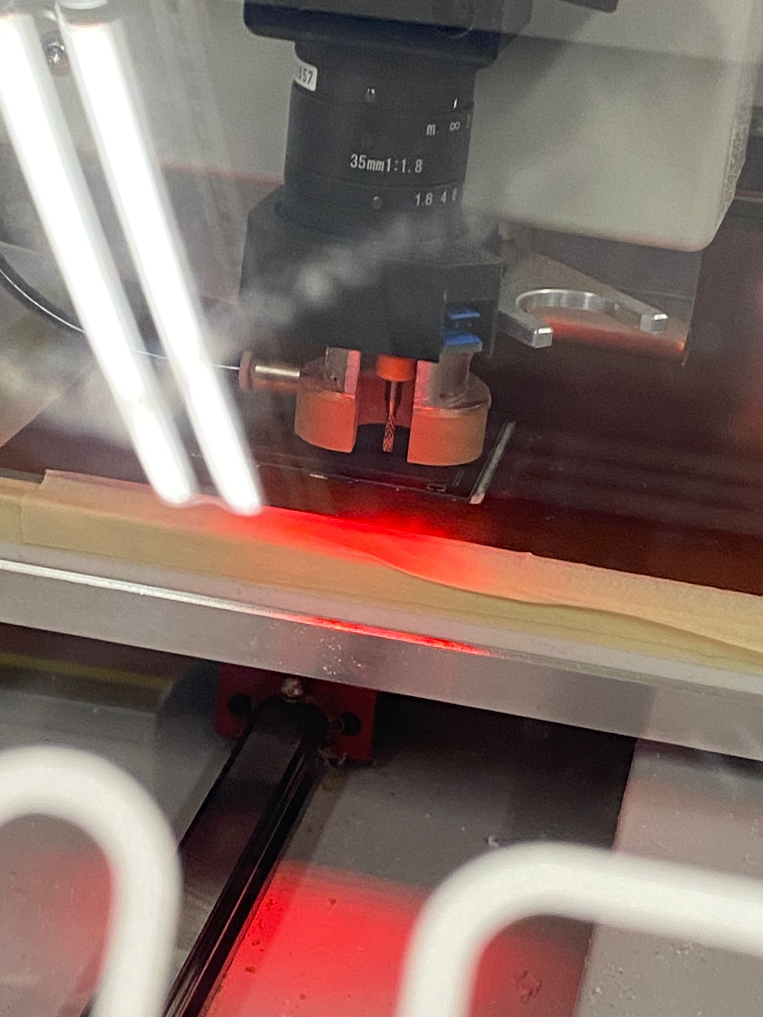
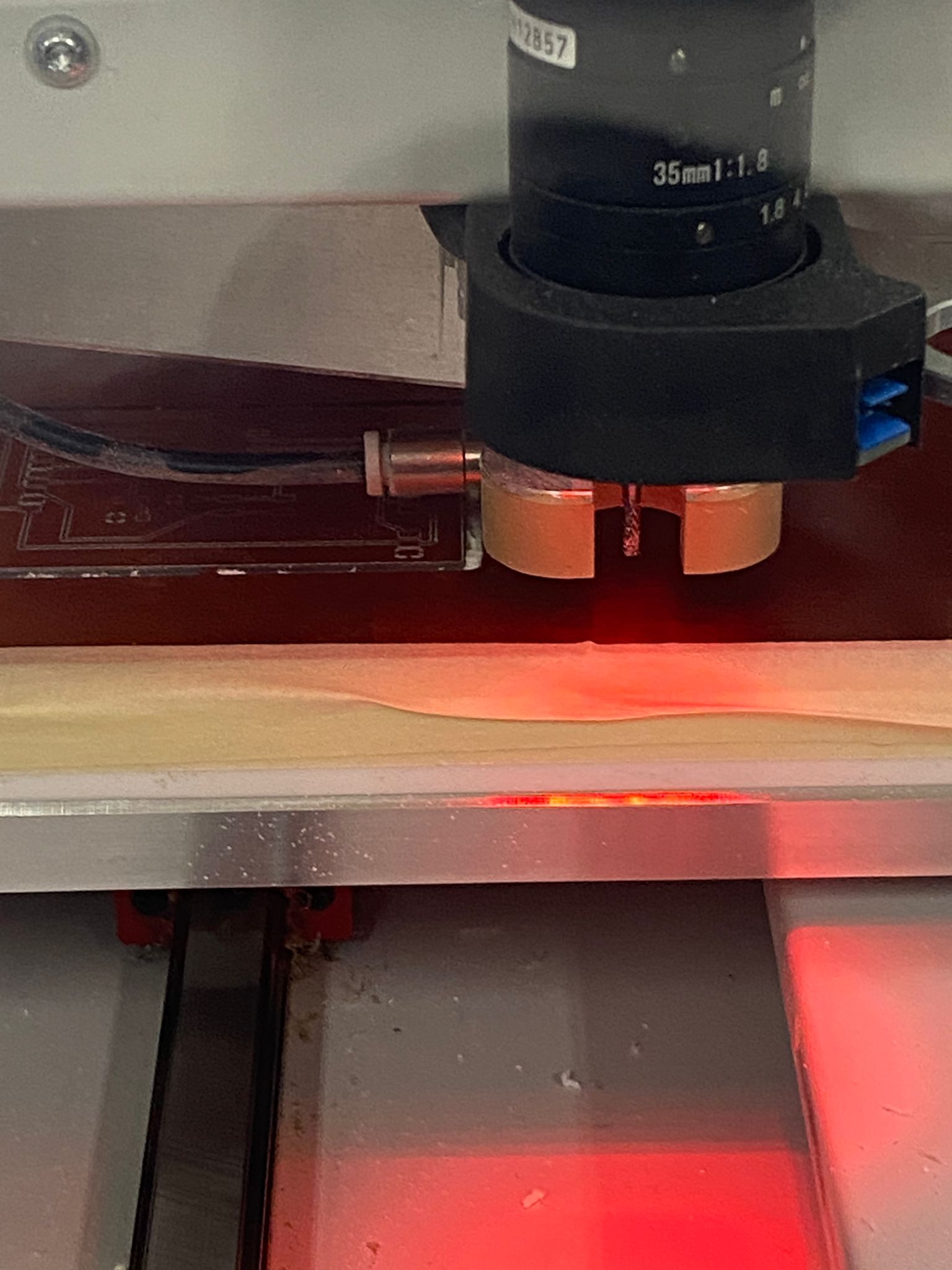
I had chosen a good corner for my design
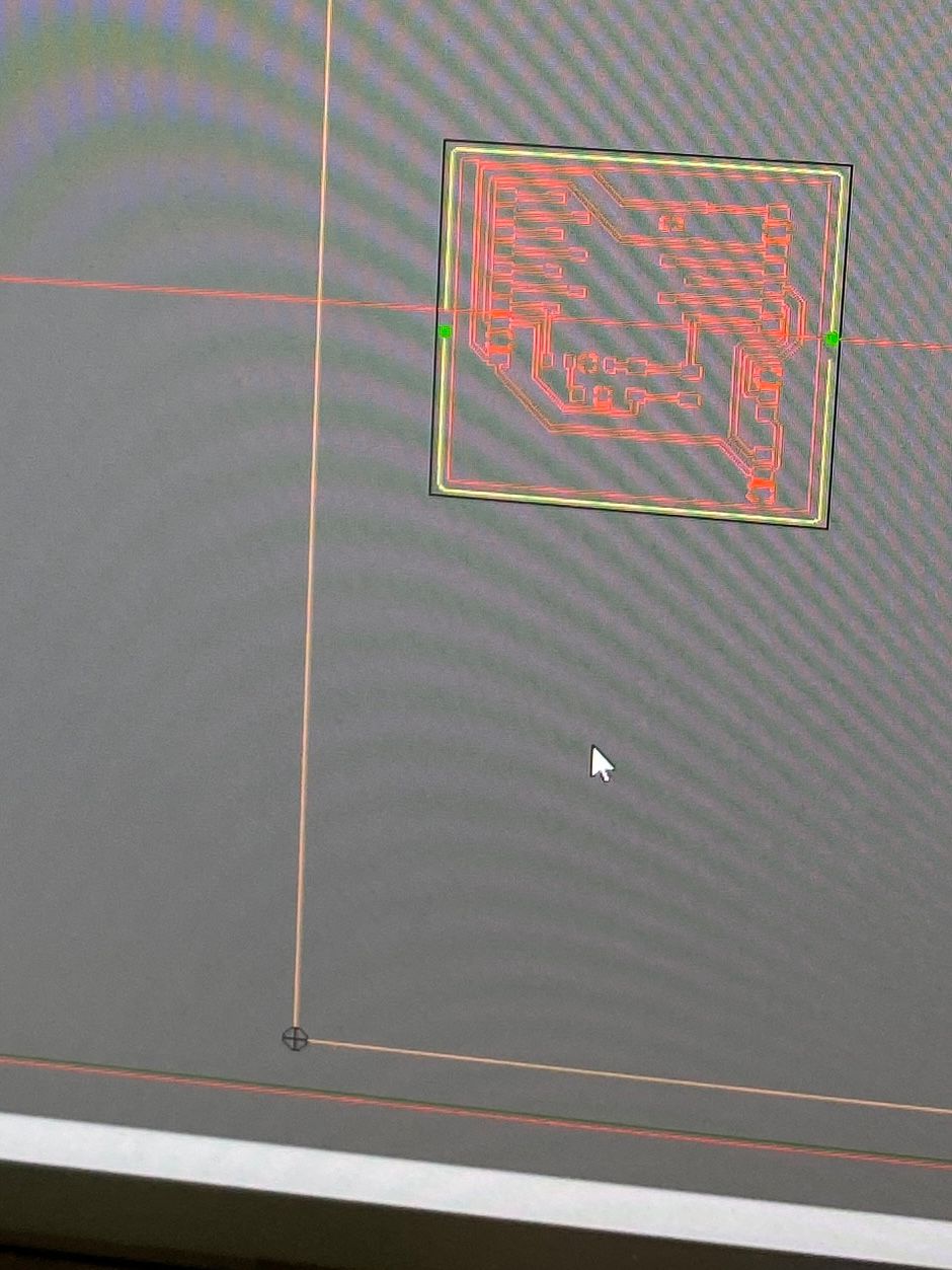 Then I adjust the location to get another corner
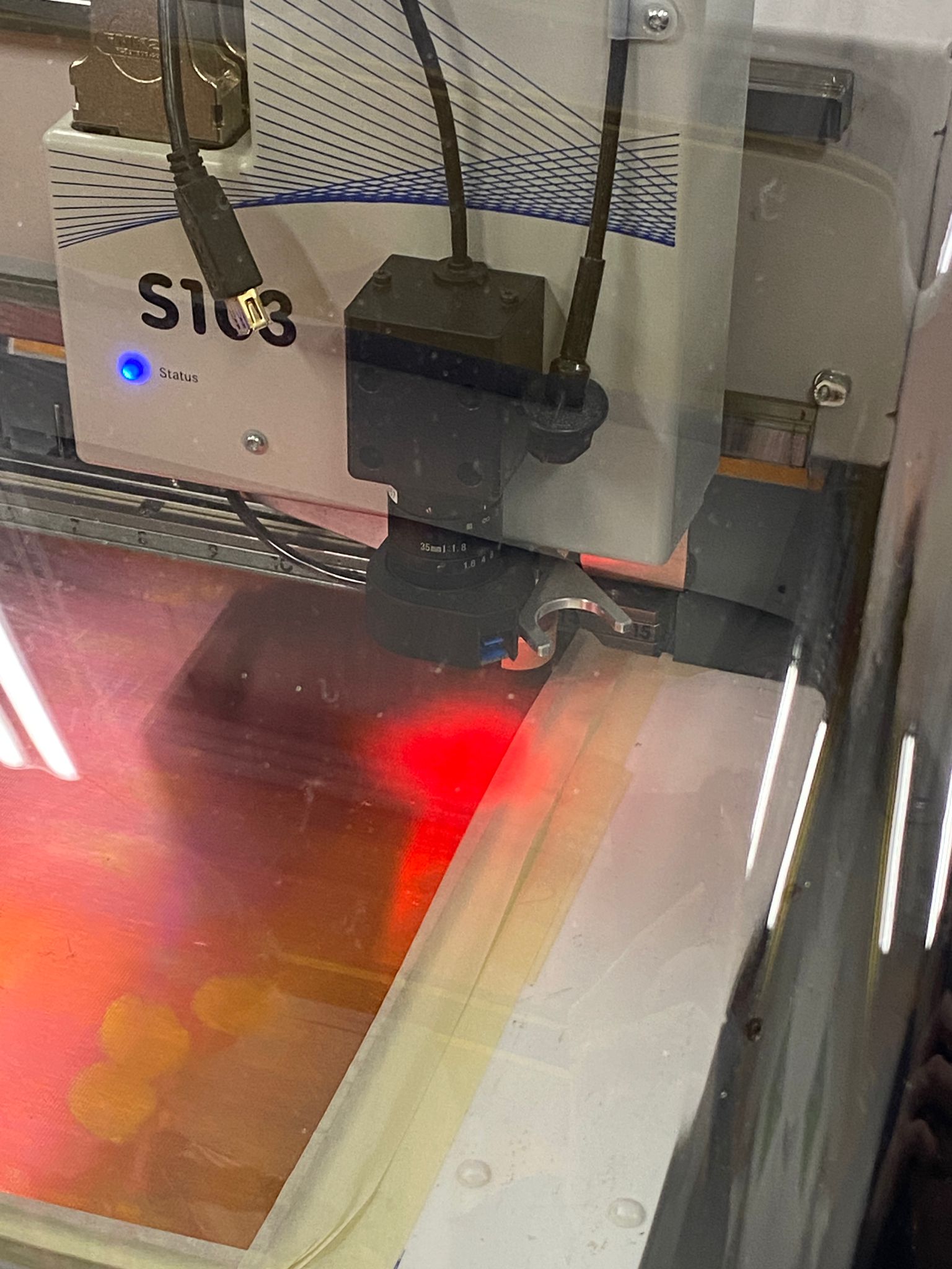
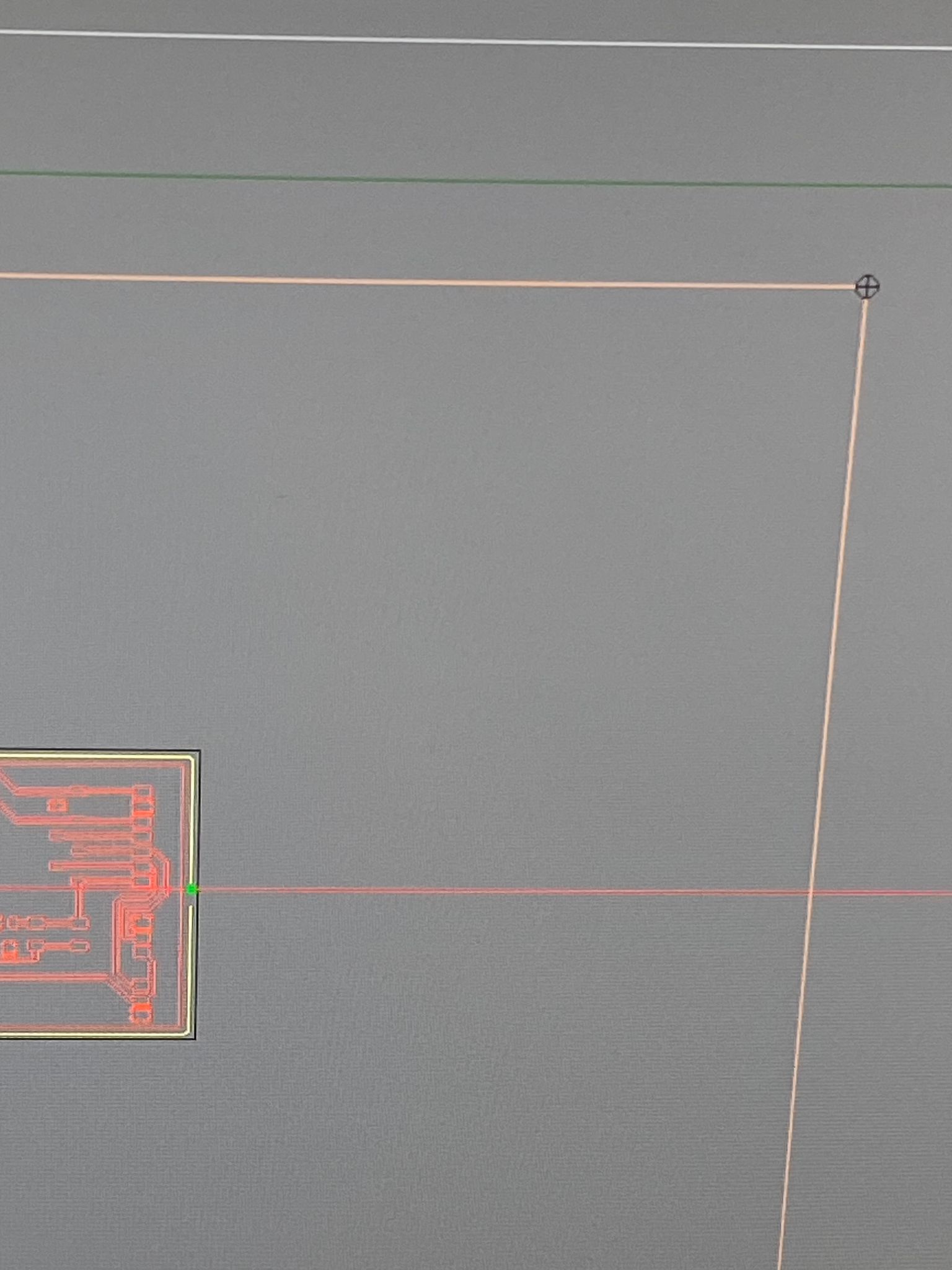
Lastly, I moved my board to a position that I wanted it to mill and cut
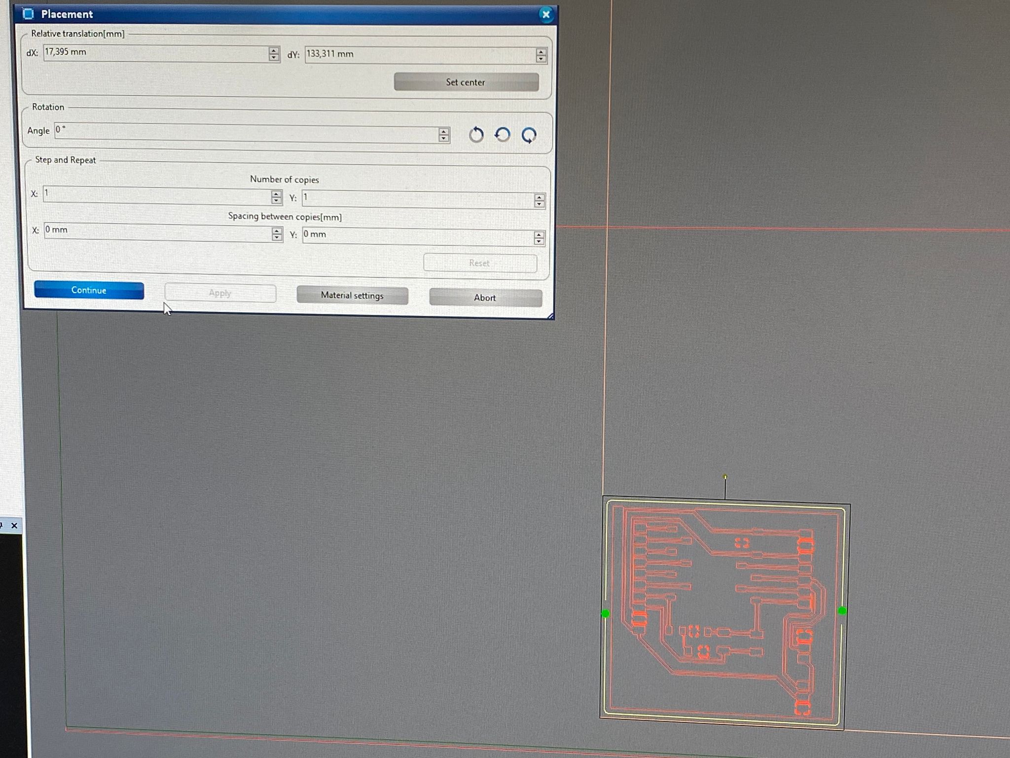
After this, the machine started milling and then cutting my circuit board. While this process occurs, I paid attention for the tools if there is a problem with changing tools in the process. Then I should stop the machine.
Last step: Vacuum the dust and remove the circuit board from the machine.
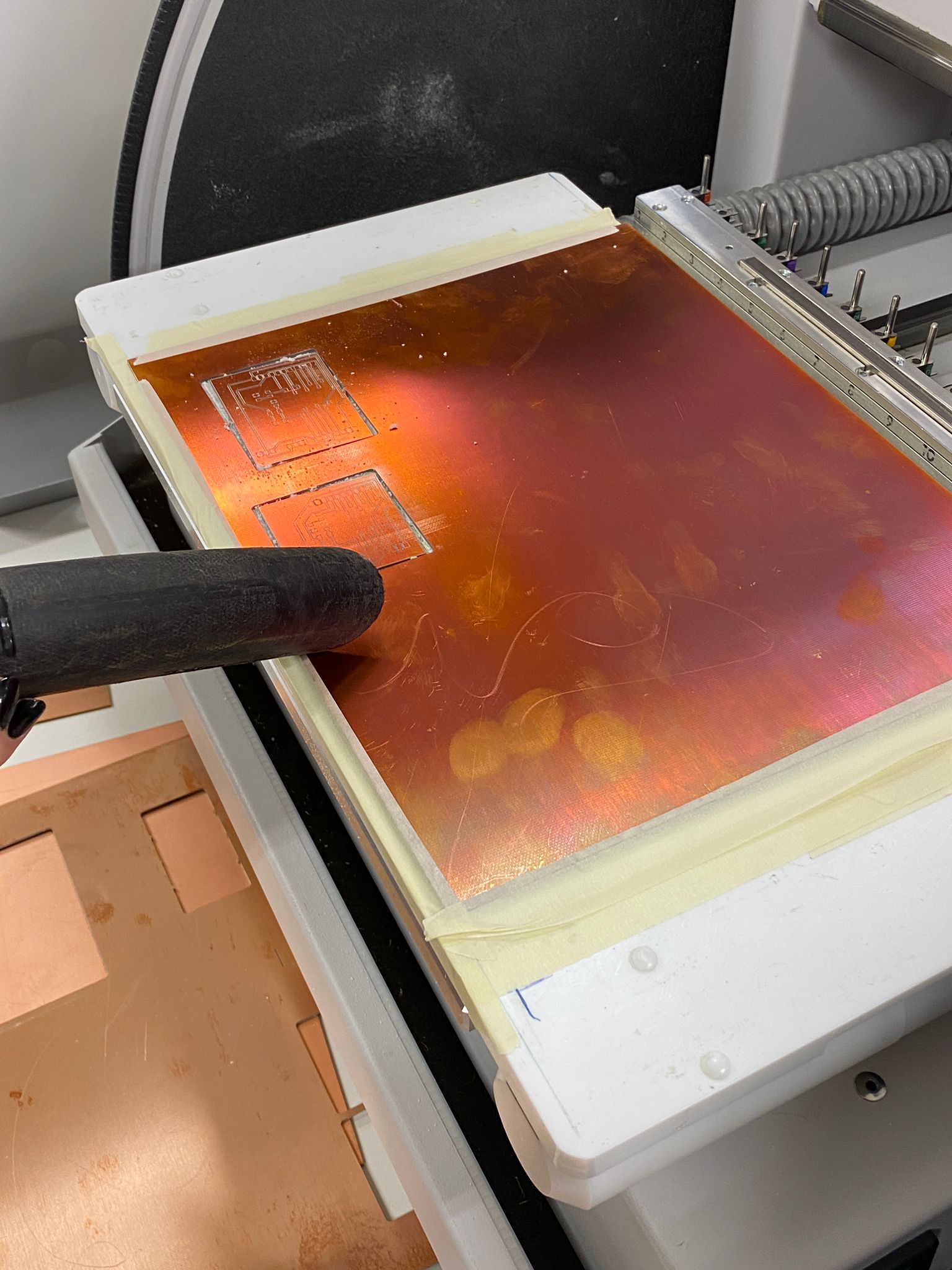
Result: Unluckily, there is a problem with my first design that the clearance between paths and GND was not clear enough so it made some short circuits at some points.
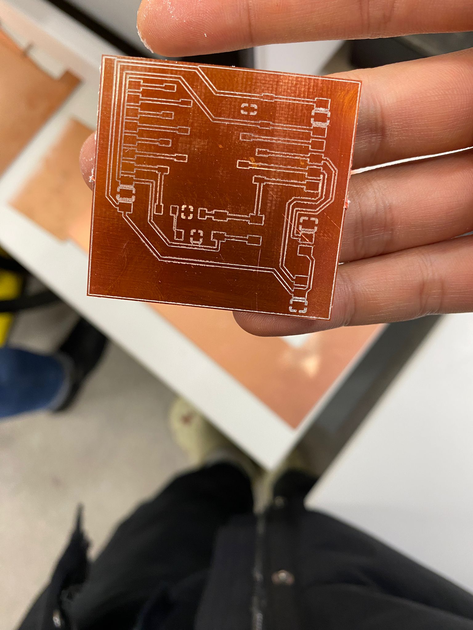
Then I changed the clearance from 0.2 mm to 0.25 mm and it worked well this time. After that, I used scouring pad to clean copper oxide layer on the top for electrical conductance.
2. Soldering components into my circuit board
Soldering microcontroler XIAO RP2040 with pins
This is the first step for me to be able to connect the microcontroller to my circuit board. The trick for this part that I used a trick tool that allign all pins to able to connect with different boards with a same microcontroller. We also can use prototype board for more common.
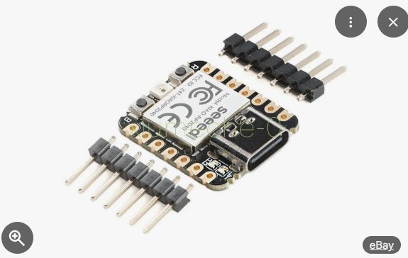
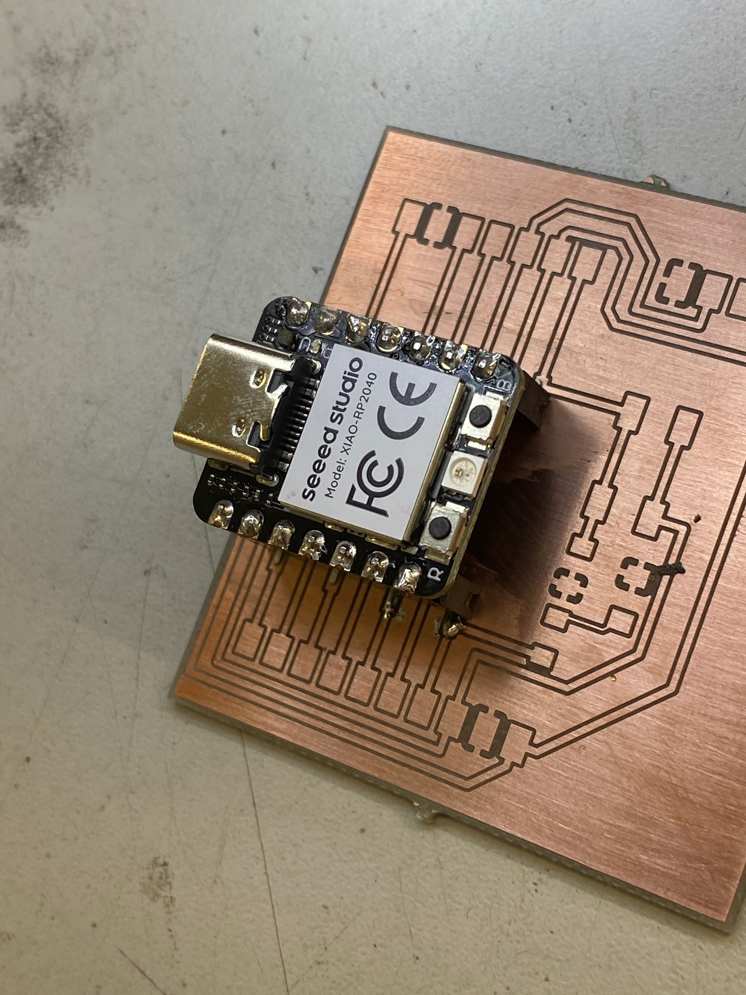
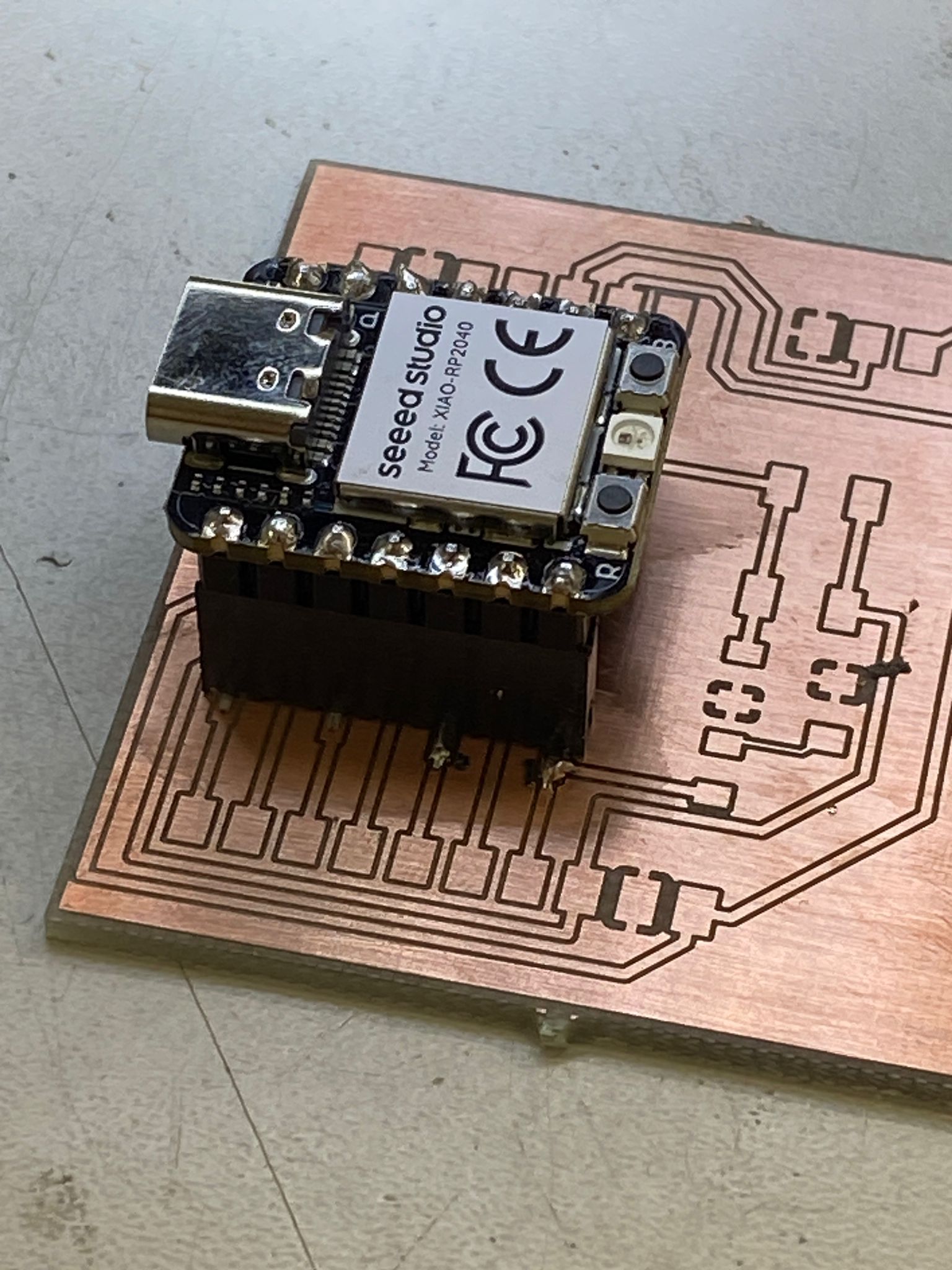
There are many techniques that can help you to solder components to the circuit board. I used pre-soldering on the connection, then I reheated that to connect them.
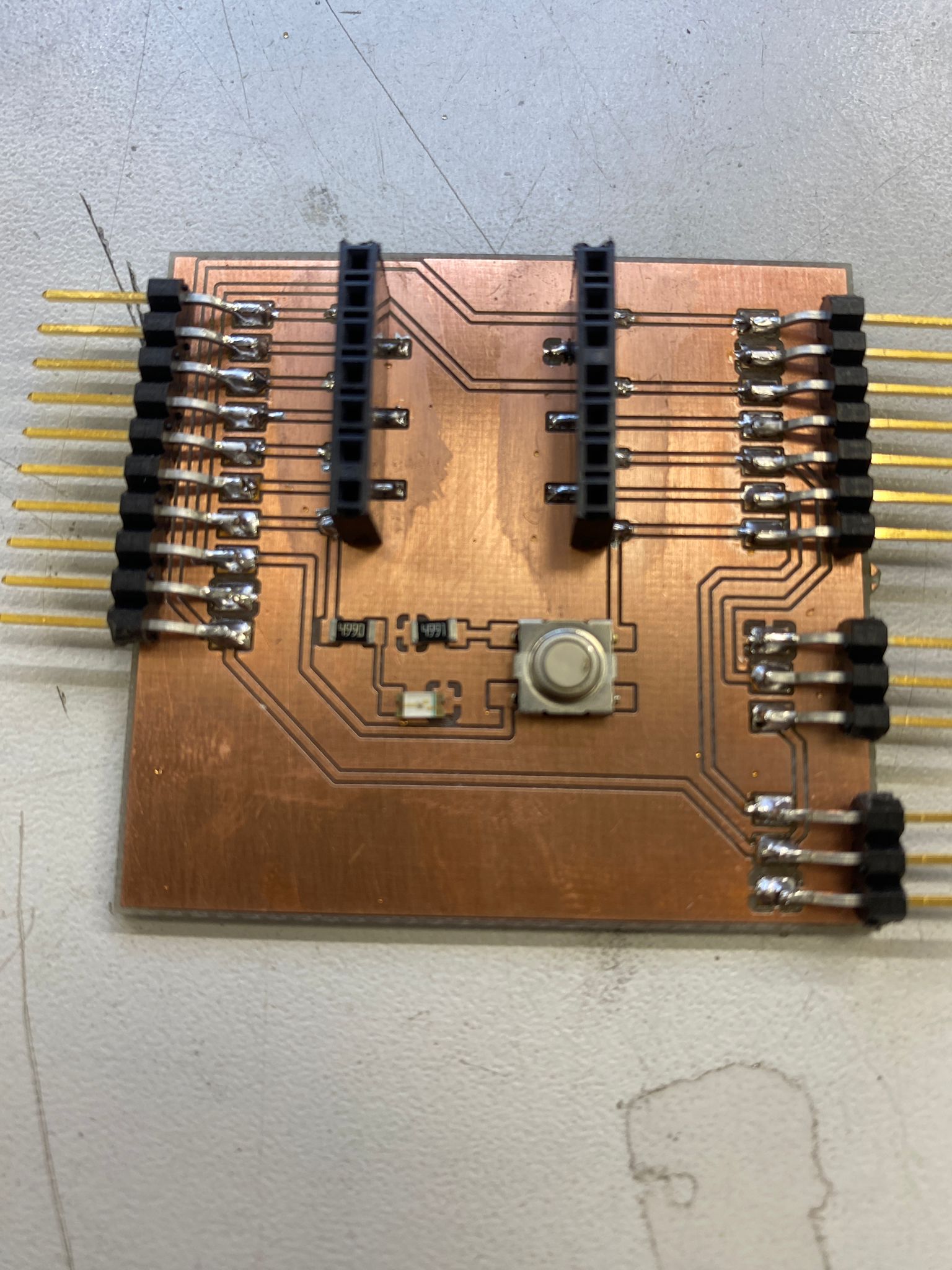
With LED, I need to measure before soldering because it is a diode. Also be careful with Ohrom twitch not to make short circuit.
Here is the final result for my design.
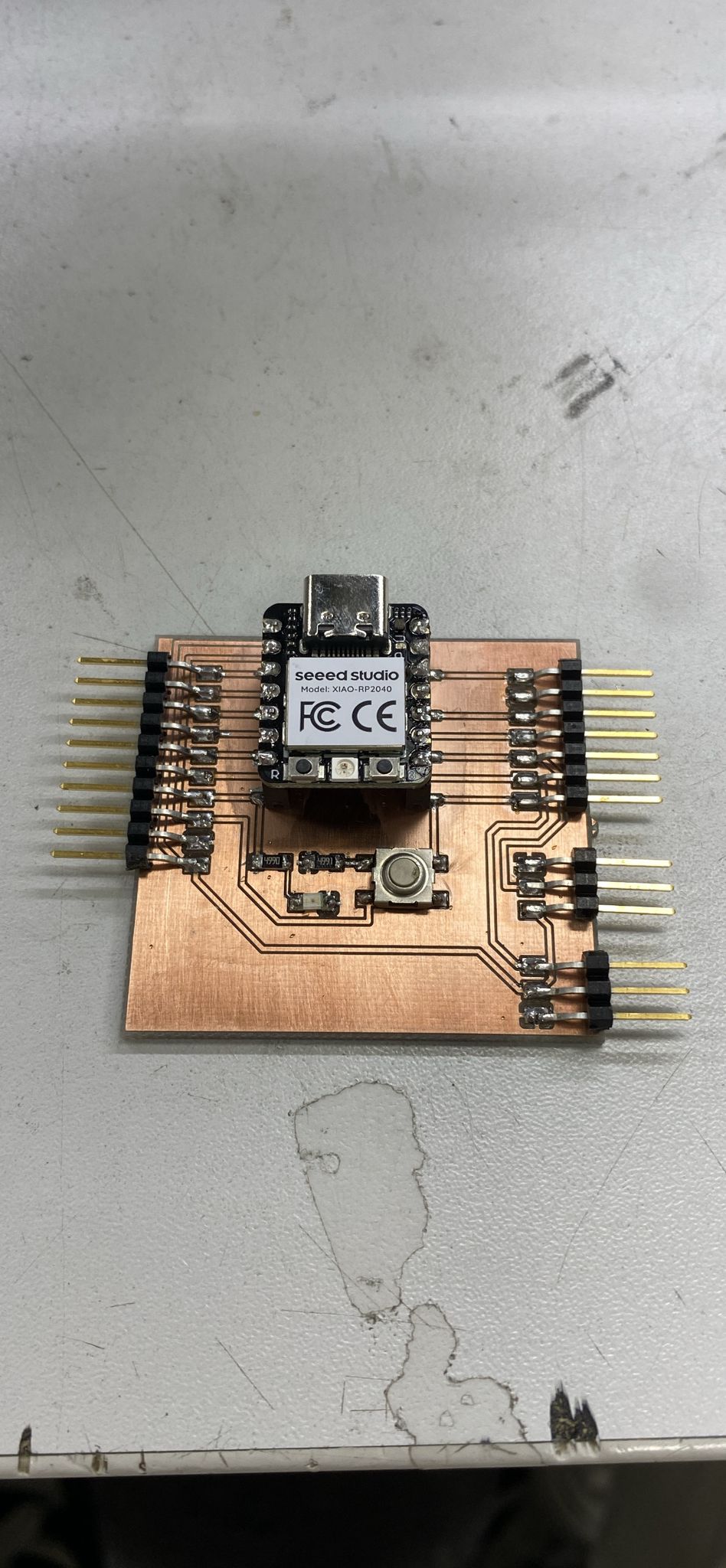
3. Testing my circuit board
Using multimeter
I used multimeter to check all my connect is good or any of them is short circuit
Using Arduino IDE
I uploaded some example codes to test the microcontroller. With Arduino IDE, I need to setup the software for the board recognization. You can find the details how to connect the XIAO RP2040 to your laptop or computer. Links
Files
Gerber F_Cu file Gerber Edge_Cuts file
Conclusion
This individual assignment demonstrated on how I milling my design circuit board, soldering components, and testing it with different ways.