7. Electronics design
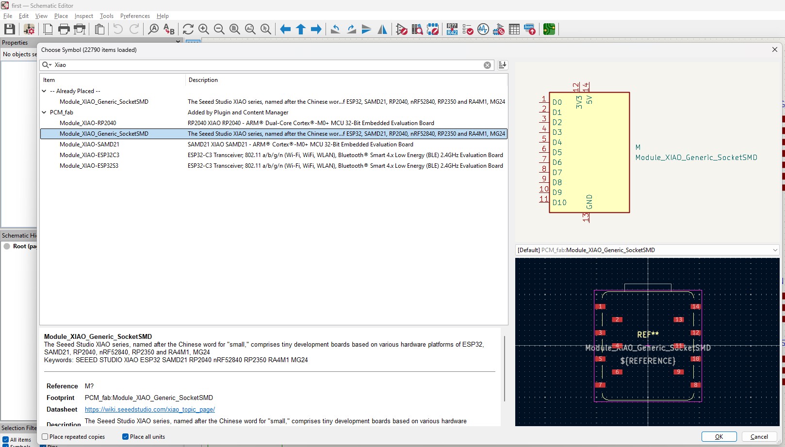
This week, I used KiCad to design a custom development board centered around the XIAO Generic SocketSMD. The goal was to create a functional system that allows an embedded microcontroller to interact with input/output components and communicate with external devices using parts available in the Fab Lab inventory.
Assignment Requirements
- Group assignment: Use the test equipment in your lab to observe the operation of a microcontroller circuit board (e.g., using an oscilloscope or multimeter).
Here is the link to our group assignment page.
- Individual assignment: Use an EDA tool to design a development board that uses parts from the inventory to interact and communicate with an embedded microcontroller.
1. Concept & Schematic Design
I chose to design a modular development board. By using a “SocketSMD” footprint for the XIAO, I can swap between different microcontrollers (ESP32 for Wi-Fi/Bluetooth communication or RP2040 for high-speed processing) without redesigning the PCB.
Component Selection (Inventory)
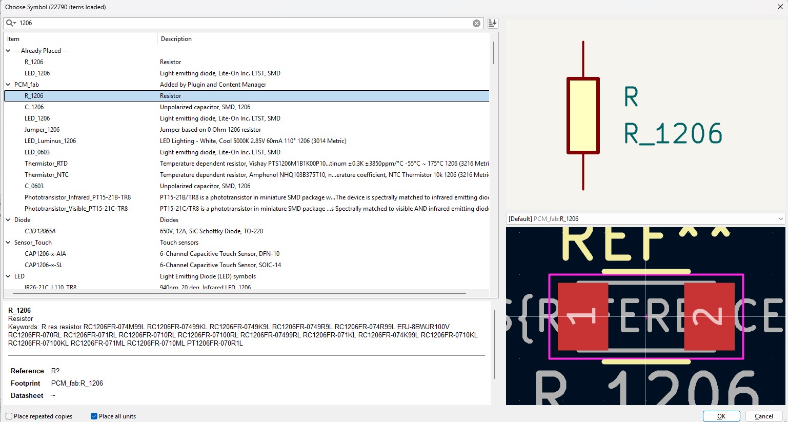
Using the PCM_fab library, I selected the following parts from the lab inventory:
- MCU: XIAO SocketSMD (Embedded Microcontroller).
- Interaction (Input/Output):
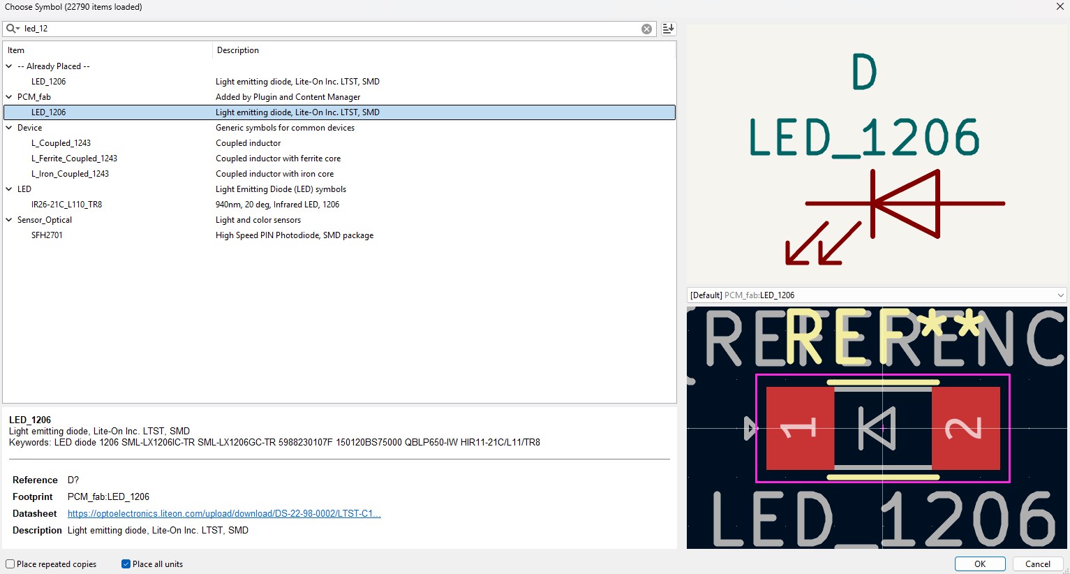
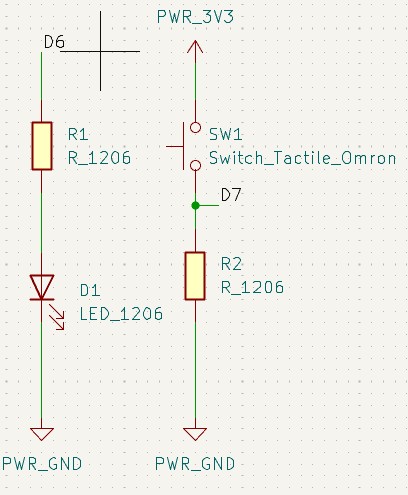
- LED 1206: A visual output to indicate system status.
-
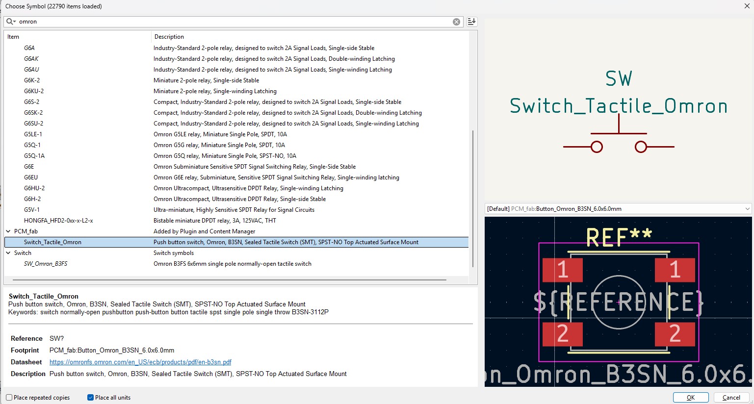
Omron B3SN Switch: A tactile input for user interaction.
-
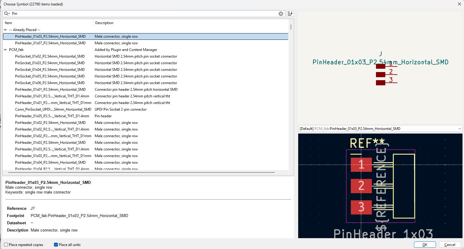
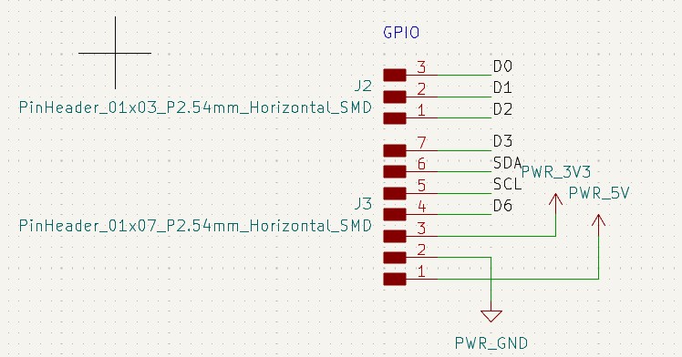
Communication: - Pin Headers (2.54mm): Used to breakout I2C (SDA/SCL) and UART (TX/RX) pins for communication with external sensors or other boards. I am using two of pinheader_1x3 and one of 1x10, but PCM_fab donot have pin_1x10. Thus, I used the combination of a 3 pinheader and a 7 pinheader.
- Passives: 1206-sized resistors.
Schematic Logic
- Interaction: The switch is connected from power 3V3 to GND with a pull-up resistor. The LED is connected to another GPIO through a current-limiting resistor.
- Communication: I exposed the I2C pins. This allows the embedded microcontroller to communicate with peripherals like OLED displays or environmental sensors using the I2C protocol.
2. PCB Layout & Design for Fabrication
Transitioning from the schematic to the PCB layout, I used “Update PCB from Schematic” button to show devices for me to wire.
Design Rules (DRC)
- Trace Width: 0.5 mm. This is wide enough to prevent the copper from lifting during soldering but thin enough to route between pads.
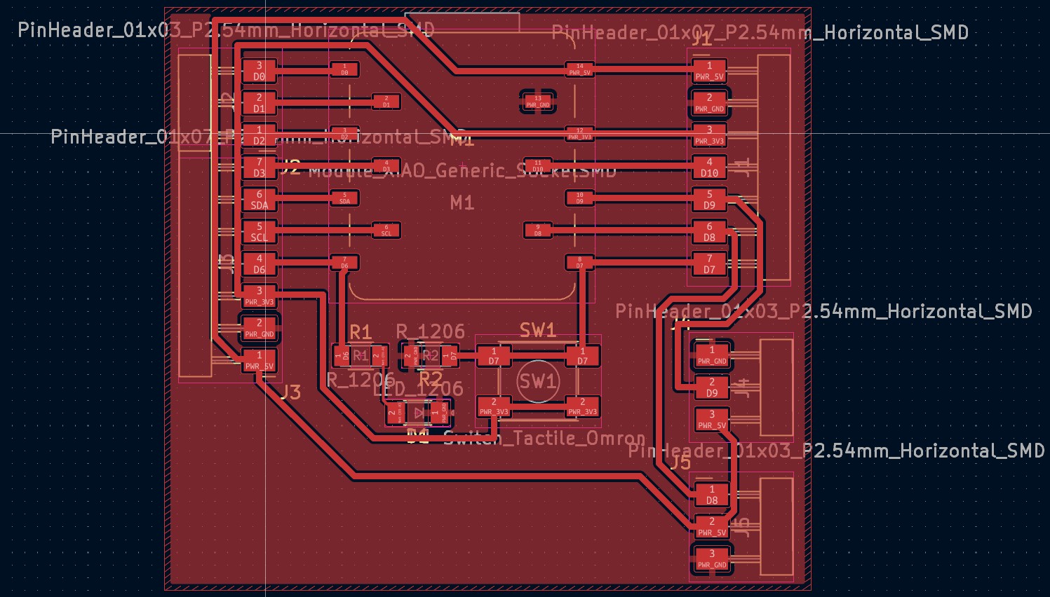
- SMD Strategy: I placed all components on the top layer. The XIAO socket is placed in the center, with headers on the edges to allow for easy jumper wire connections.
- Additional: I solve the wire puzzle with Antti’s help. I left space among GNDs because these will be automatically connected.
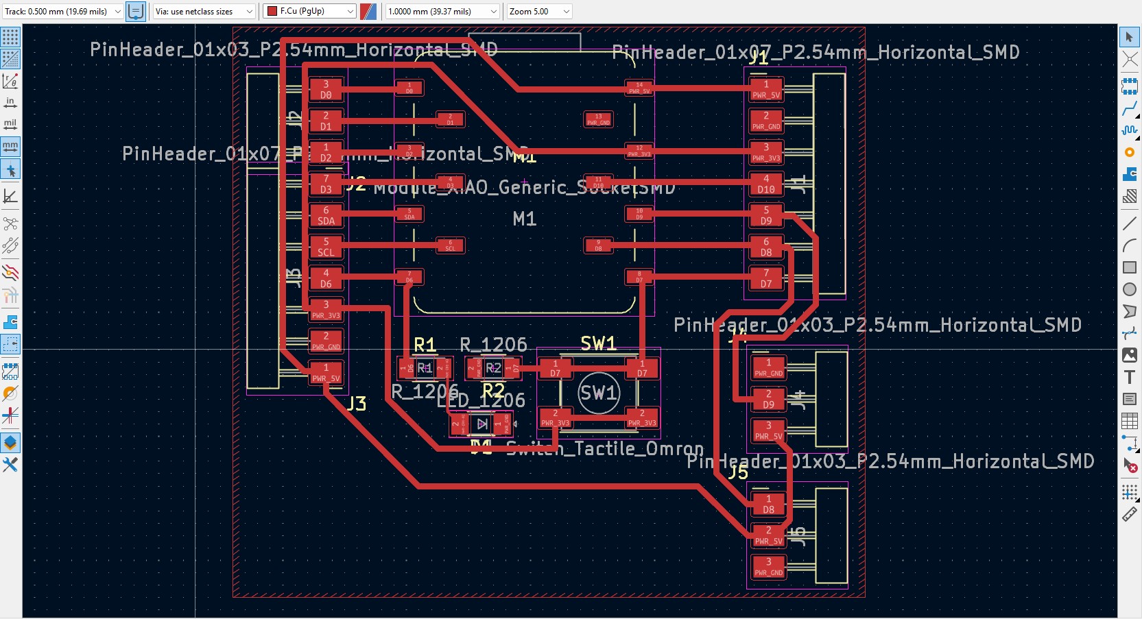
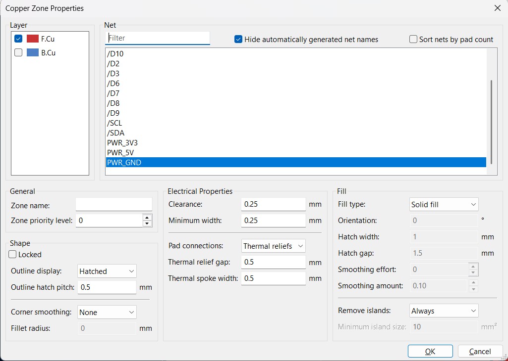
- Edge Cut: I used Edge.Cuts Layer to draw a rectangle which includes all devices inside. After that, I chose F.Cu (PgUp) Layer to draw zone fill and outline.
Here is some more properties about my zonefill.
Files
Conclusion
This assignment demonstrated how an EDA tool (KiCad) can be used to translate a conceptual interaction model into a physical circuit. By integrating inputs (switches), outputs (LEDs), and communication ports (Headers), this development board serves as a versatile platform for future embedded programming assignments.